What is Impedance?
In a circuit with resistance, inductance and capacitance, the resistance to the current flow in the circuit is called impedance.
What is Impedance Matching?
Impedance matching refers to a suitable match between the signal source or transmission line and the load; impedance matching mainly has two functions, adjusting the load power and suppressing signal reflection.
Factors Affecting Impedance
Relative to the relationship between impedance changes (one of the parameters changes, assuming the rest of the conditions remain unchanged), the factors affecting the impedance are as follows:
1. Impedance line width
Impedance line width is inversely proportional to impedance, the thinner the line width, the greater the impedance, and the thicker the line width, the lower the impedance.
2. Medium thickness
The thickness of the medium is proportional to the impedance, the thicker the medium, the greater the impedance, and the thinner the medium, the lower the impedance.
3. Impedance dielectric constant
The dielectric constant is inversely proportional to the impedance, the higher the dielectric constant, the smaller the impedance, and the lower the dielectric constant, the greater the impedance.
4. Solder mask thickness
The thickness of the solder mask is inversely proportional to the impedance. Within a certain thickness range, the thicker the solder mask, the lower the impedance, and the thinner the solder mask, the greater the impedance.
5. Copper foil thickness
The thickness of the copper foil is inversely proportional to the impedance, the thicker the copper, the lower the impedance, and the thinner the copper, the greater the impedance.
6. Differential impedance
The spacing is proportional to the impedance, the larger the spacing, the greater the impedance, and the other influencing factors are the same as the characteristic impedance.
7. Coplanar impedance
The spacing between the impedance line and the conductor is proportional to the impedance, the larger the spacing, the greater the impedance, and other influencing factors are the same as the characteristic impedance.
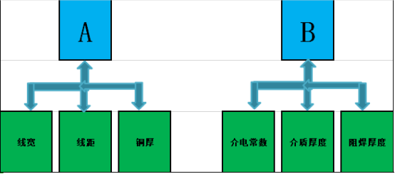
Influencing Factors of Impedance Calculation Artifact Verification
1. Production of overlay diagram
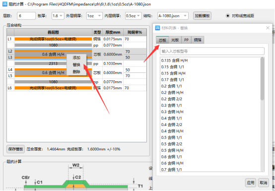
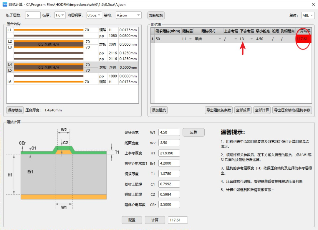
Here I recommend a free domestic tool: Huaqiu DFM software, which can automatically generate a stackup diagram, or manually fill in the number of layers, board thickness, and copper thickness, and match the impedance with the dielectric thickness of the stackup diagram.
If you need to adjust the laminate structure, the software has a library of boards, prepregs and copper foils, and you can choose according to your needs. Right-click to add, replace or delete at the parameter position where the stack structure needs to be changed. The pop-up window is the material library that comes with the software, core board, bare board, PP, and copper foil are available for selection.
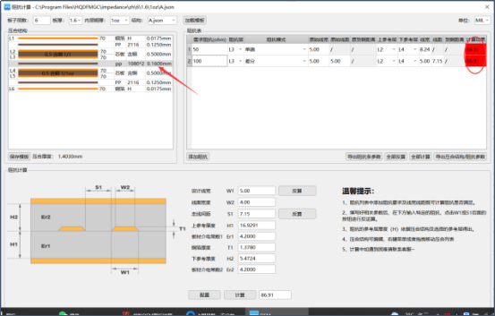
2. Effect of medium thickness change on impedance
The parameters of the laminated structure must be correct, and the parameters of the prepreg, plate and copper thickness must not be wrong. If the thickness of the plate and prepreg is used incorrectly, even if the total plate thickness can be achieved, the finished board produced by the asymmetrical laminated structure will also cause the plate When calculating the impedance, if the thickness of the medium is different from the actual production, the impedance value will be too large or too small, exceeding the required tolerance.
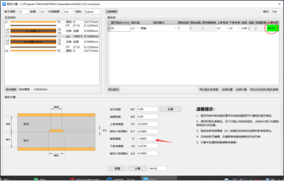
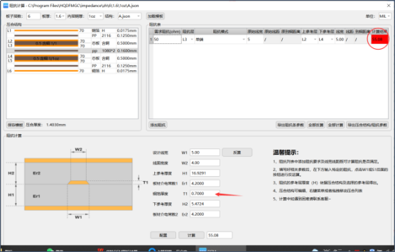
3. Effect of copper foil thickness change on impedance
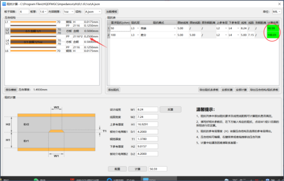
The copper thickness of the laminated structure must be selected accurately. If the copper thickness is wrong, the difference in differential impedance will be about 20ohm, and the difference in single-ended impedance will be about 10ohm. Therefore, the impedance value required by the actual design cannot be reached. For example: the copper thickness is required to be 1 oz, and the lamination is 0.5 oz. If the board is produced according to the lamination, the copper thickness of the finished product will be insufficient, and the line width will not carry enough current, resulting in the product being burnt and scrapped.
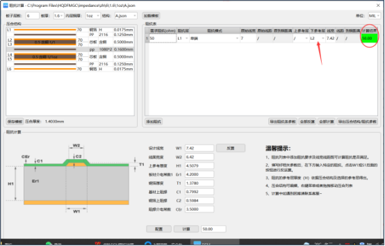
4. The influence of reference shielding layer changes on impedance
When calculating the impedance, the template cannot be selected incorrectly. The template needs to be selected according to the actual design, such as single-ended coplanar impedance. If the single-ended template is used directly, the impedance will differ by about 10ohm, resulting in an impedance out of tolerance. If it is a barrier reference, no barrier is used. The impedance of the template referenced by the layer will differ by dozens of ohms, causing the board to be scrapped directly.
 Shenzhen HongYuan Electronics Co.,Ltd