Multilayer PCBs: What Are They And Why Do We Need Them?
As technology evolves, so too do PCB manufacturing techniques. The popularity of multilayer PCBs is a testament to this trend and highlights the industry’s willingness to tailor its output to the needs of its consumers.
Join us as we explore multilayer PCBs and discover why this type of PCB is becoming one of the most sought-after designs in our field.
What is a multilayer PCB?
Multilayer PCBs are printed circuit boards with at least three conductive copper layers. They are created in a process known as lamination and typically offer greater functionality than other PCBs due to their higher-density assemblies and single connection points. Lamination consists of gluing several double-sided PCBs together with the help of suitable adhesives.
Depending on your requirements, it is possible to commission a multilayer PCB with up to 100 layers. Yet as the cost of a multilayer PCB increases according to its layers, most people opt for smaller designs. The most common number of layers for a multilayer PCB is between 4 and 12. Manufacturers prefer even numbers, as there is less chance of PCB failure further down the line.
Creating multilayer PCBs
Multilayer PCB fabrication is a delicate process in which several layers and materials are exposed to high pressures and temperatures. PCB manufacturers use a hydraulic press to create these conditions, which helps to remove trapped air when the double-sided PCBs are fused together. Common materials used in multilayer PCB manufacture include FR4, prepreg and Teflon.

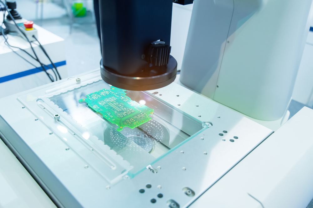
Before lamination, many manufacturers use a process known as automated optical inspection (AOI) to check each circuit board for defects. Camera-led, AOI compares each layer to the image specified in the design data. Manufacturers will make the necessary corrections if the process identifies any discrepancies. It is essential to do this before lamination as it can save substantial time and money. If issues present themselves after this point, it can often be too late to rectify them.
Multilayer PCB advantages
Because of their intricate design and production processes, multilayer PCBs are expensive to create. Luckily, they have several advantages that make these costs worthwhile. Here are some of the biggest:
Small and lightweight: With demand for portability and user-friendly devices increasing, it’s no surprise that multilayer PCBs are becoming the preferred type of circuit board. As manufacturers don’t need to worry about the connections between separate PCBs, they can create multilayer PCBs that are smaller and lighter than other types of PCBs without losing functionality. In fact, thanks to their high-density assemblies, multilayer PCBs usually have more power than either single-layer or double-sided designs.
Better endurance: Although most types of PCBs can withstand large amounts of strain, multilayer PCBs are a different breed. Because multilayer designs need to deal with high pressures and temperatures in their creation, they are naturally more durable. This increased resilience ensures a longer lifespan than most single-layer designs, as do their multiple layers of heat-protective insulation.

Increased power: Where single-layer PCBs can only do so much, the increased surface area of multilayer PCBs enables them to achieve greater functionality, capacity and speed. With more layers and better connectivity, multilayer PCBs are also much more reliable than other PCBs. These traits have made it possible to include higher-capacity PCBs in smaller devices with minimal effort.
Single point of connection: As they are single units, there is no need for multilayer PCBs to connect with other PCBs. This helps save space within devices and will reduce the risk of problems at any point in the product's life.
 Shenzhen HongYuan Electronics Co.,Ltd